Peek use in Semi-Conductor Applications – Wafer Manufacturing
February 7, 2023 | Blog, Industries Blogs, Materials Blogs, Peek Materials Blogs
PEEK is short for polyether ether ketone. These polymers are notable for their phenylene rings and oxygen bridges, which result in resilience, durability, and strength.
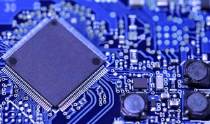
Wafer manufacturing is a term used to describe the process of creating chips, otherwise known as integrated circuits, which are used in everyday devices. You will find chips in everything from cars to military jets. PEEK is great for semiconductor applications because of its outstanding combination of physical properties.
- Longer Lifetime – CMP (chemical-mechanical positioning) rings made with PEEK can provide less downtime, and more throughput with up 2x wear resistance compared to other materials.
- Potential Yield Enhancement – Low particle generation and higher purity, resulting in lower outgassing and extractives that may lead to yield improvements
- Faster Process – PEEK endures proceseess with up to 260° and harsh chemicals, which allos for faster processing and less cooling time.
Semiconductor equipment manufacturers use PEEK screws and fasteners in wet benches. Chip manufacturers use hydrofluoric acid which is a corrosive chemical that can damage metals. Since PEEK is chemical-resistant, chip manufacturers are utilizing PEEK screws. These screws are used in the production of ICU’s since they are a high-purity material and possess low-outgas properties. PEEK is also used to manufacture manifolds for semiconductor production equipment.
Performance Plastics’ team of experienced engineers possess the expertise to design and manufacture technically challenging projects and offer complex solutions within the semiconductor industry.
For more information on how Performance Plastics can assist in your material selection challenges, please contact Rich Reed, VP Sales & Marketing at 513.321.8404 or [email protected].